Place of Development: University of Buenos Aires - Faculty of Engineering
Date: November 2009
Duration: 6 weeks
Author: Pablo Manuel Delgado et al.
The main objective of this project was to get familiarized with the aspects of constraints, design, simulation and implementation of a discrete component low distortion professional audio power amplifier, from scratch. This took place within the course of Analog Circuit Design at the University of Buenos Aires. The total time given for the project was approximately four weeks, during which all the stages -design, implementation, quality control and measurement- took place.
The work itself had as a second goal to strengthen multidisciplinary work, given the eclectic formation that the University's engineering students have. The project had well defined deadlines and staff/client meeting directives that had to be accomplished by any means.
The project itself consisted on mainly three parts: design, implementation and measurement. This order is not necessarily followed since there always exists a certain amount of feedback between the modules, consisting of stages of revision, recalculation and redesign.

The design part is mainly divided into the three fundamental circuit blocks comprised in any professional audio amplifier, along with their initial block statement, main functionality and subsequent improvements.
The simulation part consists on the verification of the analytical calculations and the justification of the chosen parameters, as well as the component types. Another good use of the simulation is to provide fast methods of calculation for a posteriori component value and signal parameters over the three stages. One of the main examples of this method is the determination of the miller capacitor compensation, where an analytical calculation can be rather tedious, considering the intricate circuit topologies and the closed feedback loops that can be used.
Many measurements were taken later as to confirm the design stage procedures and simulations.
The design stage also comprises a set of well known practices for thermal protection and control, grounding, connector placement, ripple attenuation filters, cost and component technology.
Index
Design
Input stage
Differential Pair
Input Stage Circuit
Input Impedance, Offset, Noise Immunity, Buffer Circuits
Voltage Gain Stage
Improvements to the first approach.
Voltage Gain Circuit
Preliminary calculations. Open loop gain.
Output Stage
Initial statement
Improvements
Output Stage Circuit
Global Feedback
Frequency compensation, Slew Rate and Miller Capacitance correction
Complete Circuit
Simulations and Measuring
Bias Voltages
Voltage Gain
Output Power
Power Bandwidth, Slew Rate, Rise Time
Input and Output Resistances
Phase Margin and Frequency Compensation
Distortion Figures
Overall Comparison
Prototype Implementation
PCB Design
Grounding
Filtering Capacitors
Signal Path and Power Path
Heat sink calculation
Component Technology
Design Parameters
Output Power: > 20 W over an 8 Ohm load, 1 kHz and a THD < 0.1%
Support for 8 Ohm and 4 Ohm loads.
Total THD < 1% from 20 Hz to 20 kHz with 1 W over an 8 Ohm load
Bandwidth from 10Hz to 100Khz with 1 W over an 8 Ohm load
Power bandwidth > 20 kHz
Damping factor over 200
Input impedance > 50 kOhm
Output offset voltage < 20 mV at room temperature
Power consumption < 5W without signal
Short circuit protection at the output stage
Input stage
The main role of the input stage is to generate an error signal by subtracting the feedback signal, as well to present a high input impedance to the signal generator and provide common mode noise immunity Lastly, it is also important to have a certain voltage gain for better inter stage adaptation.
One of the main design parameters is the stage's transconductance, given by the power bandwidth required on the amplifier. A way of having a certain control over the amp's frequency response is to provide a dominant pole. It is convenient then to connect the capacitor providing this pole as a feedback loop between the input and the output nodes of the voltage gain stage (second stage), which is next to the input stage (first stage).
The reasoning is as follows:
Consider the output current of this first stage \( I_{out} \) as the one which charges this dominant pole capacitor. Given a desired bandwith of \( \omega =2\pi*20kHz \) and considering a capacitor value \( C_{dom} \) between 50pF and 100pF, we have the following relation:
\begin{equation}
I_{out} = w*C_{dom}*V_{max}
\end{equation}
where \( V_{max} \) is the maximum voltage value, deduced from the fact that the max. power (20 W) for the amplifier is \( P=V_{max}*V^2/8 \Omega \). Using (1) we can estimate an order of magnitude for the current of the input stage (1 to 3 mA). This bias current must be enough to grant the correct transfer capabilities and induce the stage to a linear operating mode.
Regarding circuit topology, an apt transconductance amplifier for this stage would be, at a first glance, a common emitter configuration, possibly with an emitter degeneration resistor to improve stability without compromising the desired transconductance. The transistors were chosen to be Bipolar Juncture (BJT) due to a better current amplification factor \( \beta \) than the Field Effect ones. Also, care must be taken in the values of the impedance input given by the devices (much higher in MOSFET and JFET) as to not to degrade thermal noise input immunity.
Differential Pair
Even though a BJT common emitter configuration -with the correspondent improvements- would accomplish the previous requirements, there are other needs to be satisfied as well. The inclusion of a differential input stage give the following advantages:
- An entry point to the closed feedback network, capable of subtracting the sensed output signal to the input signal for an improved stability. This added transistor presents a high impedance node to the feedback network, giving the chance to use feedback network capacitors of lesser values. The feedback signal is also emancipated from the input signal, providing noise immunity due to possible noise present on the circuit's power rails.
- It's high symmetry provides improvements of the offset voltage and consequently a better offset for the output stage, which is very desirable if decoupling capacitors are not used at the output.
- Common mode rejection.
Nevertheless, the inclusion of a differential input stage brings along some undesired effects, such as inter modulation and harmonic distortion due to a possible pair unbalance. This is the main reason why other modifications must take place in other parts of the circuit in order to maintain the desirable advantages provided.
Chosen Circuit
 |
| First Stage - Signal Conditioning |
|
This is the final topology chosen for the input stage. Each of the component values were chosen to optimize the effects mentioned above.
- The differential pair was implemented by transistors Q1 and Q1 and the model 2N3906 was chosen due to its good noise immunity and a relatively high current amplification factor
- The active load given by Q8 acts as a current source with the reference voltage given by the diodes D1 and D2. It's purpose is to provide a stable bias current to stabilize the value of \( G_m \), the value of the stage's transconductance. This is done so to avoid any potential sources of distortion, and it's much better than the sole use of degenerating resistors due to possible variations on the bias current.
If we suppose the diodes generate a voltage drop of approx. 0,6V and a transistor base-emitter juncture drop of 0,6 as well, along with the 470 \( \Omega \) resistor, it can be seen that the current on that branch must be around 850 \( \mu A \). This current is more than enough to guarantee a good linear transfer and the bandwidth requirements. In fact, the 470 Ohm resistor was chosen to give some room to experimentation with different component values in a less restrictive environment.
- The transistors Q3 and Q4 provide also a greater balance to the differential pair and duplicate the total transconductance. Degenerating resistors were chosen as to provide a voltage drop of around 60 mV and better means of stability.
The inclusion of a mirror current source for pair balancing induces a better second harmonic rejection (and thus distortion rejection) of the resulting signal due to the counter phase summing. The doubled transconductance implies a better linearity for input signals with doubled amplitude, and due to the quadratic dependence of the stored energy, the distortion performance improves by a factor of 4 in total.
- Resistors R1 and R2 correspond to degenerations on the differential pair emmiters. It can be shown that the differential pair gain is given by
\begin{equation}
G_m = \frac{g_m}{1+g_mR_e}
\end{equation}
where \( g_m \) are the individual transconductances of each of the pair branches and \( R_e\) its corresponding degeneration resistors. This is of course a local closed loop feedback equation and thus a mean of stabilization. There is a tradeoff between the value of \( G_m \) , resistor values and the capability of stabilization vs noise immunity. Linearity becomes more difficult to achieve with greater resistor values.
Input Impedance, Offset, Noise Immunity, Buffer Circuits
The amplifier's input resistor (R26) can be defined arbitrarily due to the fact that the Thevenin equivalent viewed from the input transistor's base is practically \( \beta \). If we also take into account the total feedback, the input resistance will be even higher. Even though a high value is required, there is a trade-off between source independence and noise immunity.
This amplifier is to be designed under the premise that only low impedance sources will be used to drive its input. This is due to the fact that an output impedance comparable with that of the input could make the amp's lower frequency response dependable of an external parameter, since there is a dominant low frequency pole located at that node. Besides, the voltage transfer could be insufficient for the correct operation. If one is to be working with sources of very different input impedances, a buffer circuit should be used (bootstrap or input opamp).
A last, but not least, thing to take into account is the fact that the polarization current can destabilize the pair's bias symmetry when flowing through the input resistor, so the total resistance seen by the base of the other transistor in the pair (Q2) must be equal to that seen by the base of (Q1), i.e. R26. The calculation of the total current gives then:
\begin{equation}
I_{outmax} = \frac{I_{pol}}{2} \approx 0.5 mA \mbox{ } to \mbox{ } 1.5 mA
\end{equation}
A value that clearly accomplishes de a priori calculation to guarantee the desired power bandwidth.
voila!
Voltage Gain Stage
The main functionality of this stage is to provide a good value of open loop voltage gain to properly apply a closed feedback stable loop. By doing this, the amp's behaviour can be independent of external parameters and internal gain fluctuations due to bias current drifts and other effects. One must hereby take advantage of all the premises taken into account on the design of the previous stage, as to avoid as much as possible any additional sources of distortion.
The core of this stage is no other than a common emitter with subsequent improvements for linearity and stability. This part of the circuit must be capable of producing the maximum voltage swing without limiting, given the power specifications, with a rather large equivalent impedance in order to drive the output stage.
Another important aspect of this stage's design is the placing of a dominant pole by means of a capacitive feedback loop. A different explanation for the so called Miller capacitor is given, from a circuit analysis point of view that matches the one given by classical control theory.
The miller capacitance must be such that it can generate a time constant sufficiently large enough to provide a dominant pole that controls the amplifier's total frequency response. The actual value of the local feedback capacitor is then "mirrored" to the base of the main transistor, multiplied by the stage's equivalent voltage gain. This way, a capacitor with a low value can have an equivalent value of many times its order of magnitude, so to facilitate the pole placing.
The question arises as to whether this is necessary at all. Given the great drift in \( \beta \) values of BJT transistors, this also leads to distortion in the total voltage gain of the amplifier. One of the main purposes of design engineering is to take this sort of uncontrollable variations and make them negligible, and this is thus the main reason for the controlled placement of the dominant pole, by translating these variations over to frequencies outside the range of operation.
In a general perspective, the Miller capacitor provides a local high frequency stabilizing feedback whilst the global feedback network provides stabilization amongst the low frequencies.
A well designed voltage gain stage should not be a major source of distortion or signal degradation as to be seen below.
Improvements to the first approach.
A second stage corresponding to a common emitter configuration can be improved as following
- Even though the Miller capacitance reflection can be enlarged by means of augmenting the stage's voltage gain, another efficient way of achieving this is to enlarge the time constant by including a previous adaptation stage (buffer), to rise the total equivalent resistance seen by the capacitor at the input.
- A transistor with good current driving capabilities is also recommended as well as a current protection.
- An emitter degeneration can be introduced to raise stability
Circuit
 |
| Second Stage - Voltage Gain |
|
- The core of this stage is given by transistor Q6, model BD135 BJT NPN chosen because of is relatively high current gain and current drive capabilities (approx 6W)
- The local feedback capacitance given by C3 is approximately 100pF by design (normalized to two caps of 47 pF each) Note: The value of this capacitor was of 47pF a priori, giving a phase margin of 60 degrees by simulation and then corrected on the assembled prototype as some high frequency oscillations were still observed due to de-compensation.
- Transistor Q5 adapts the impedance mismatches between the first and the second stages. Its configuration is emitter-follower, so the total voltage gain \( A_v \) is due mostly to the second transistor. Nevertheless, the value of C3 can be reduced even more as explained above due to this addition. The total resistance seen by the Miller capacitor is \( \beta \) times greater (beta enhancement technique).
It is necessary though to establish a trade-off between a proper dominant pole value $$RC_3^* = RC_3(1-A_v)$$ and an according slew rate.
- Transistor Q7 acts as a current oveload protection with the 47 Ohm resistor calculated to produce a 0.6 v activation voltage drop against a 12 mA current.
- The ensemble of the two 47 Ohm resistors R6 and R7 correspond to a local feedbaxck by means of emitter degeneration for \( A_v \) stability when the current protection is not active.
The distortion due to alinearity and load resistance variation is then covered.
Preliminary calculation. Open loop gain.
Given a Darlington configuration comprised of Q5 ( \( \beta_5 = 150\) ) and Q6 ( \( \beta_6 = 130\) ), the total transconductance can be calculated as:
\begin{equation}
G_{m2} = \frac{g_{m2}}{1+\frac{r_{\pi1}}{(\beta_5+1)r_{\pi2}}}
\end{equation}
This calculation was quickly carried out in Mathcad, giving the following results, given a nominal bias point current of 5mA:
 |
| MathCAD caption for Gm calculation for a nominal current of 5mA. |
|
This value of Gm = 170 mA approx was confirmed by simulation. This gives an open loop gain of
\begin{equation}
A_{vol} = \frac{G_{m2}R_c}{1+G_{m2}R_c} \approx 220
\end{equation}
where \( R_c \approx 20 k\Omega \) is in this case the estimated equivalent input resistance of the third stage, and thus the equivalent load resistance of the second stage.
Output Stage
Initial statement
The output stage is perhaps the most important in the design of a low distortion amplifier, as it is the source of many issues regarding this subject. Its primary function is that of achieving a good impedance adaptation between the final load and the voltage gain stage, by providing sufficient current driving capabilities. This also has to be done in the most efficient way as possible. In general, these stages do not provide additional gain factors.
Due to efficiency concerns, the implemented output stage will be of Class AB. This means that there will be a complementary transistor configuration that will drive each a half a cycle of the current signal. This offers basically a better energy efficiency, due to the fact that the whole linear swing range of each complementary device is used for only a semi cycle of the signal.
As usual, a trade-off is to be taken into account between complexity and efficiency:
- As every power stage, this one will be operating under great temperature constraints due to large current amounts on the devices' junctures, so a thermal tracking system for compensation effects must be implemented.
- There is distortion due to the zero crossing of the signal and the switching of each semi cycle.
- Charge decoupling is necessary by a method other than capacitive decoupling, due to the great power constraints on these nodes.
- As a consequence of the great temperatures, a dissipation device must be calculated and properly installed. Mechanical design principles and thermal transfer laws are taken into account in order to preserve the semiconductor devices.
- Another desirable element is a system of (short circuit) current protection in case of a collector current greater than the maximum specified by the semiconductors' datasheets.
Improvements
Many alternatives were proposed to tackle these issues:
- A split power supply scheme (+/- 24 V) can be used in order to avoid the use of decoupling capacitors at the output stage. With a correct calibration of the input differential stage and the output stage's offset voltage a very good level of bias current attenuation can be achieved for load decoupling. Also, this scheme allows the saving of some bias components such as ground pulling resistors.
- Thermal tracking is achieved by a base-collector voltage multiplier circuit, similar transistors to those employed in the output stage are used in order to have a similar temperature response behaviour.
- To improve this stage's beta drift stability degenerating power emitter resistors will be used, these ought to be of a low value due to the great currents that flow through.
- Current protection will be implemented with a transistor-resistor configuration accordingly calculated
- As seen in the previous section for the second stage, the inclusion of a Darlington configuration on the output stage also ameliorates the stages input and output resistance, as well as the transconductance
Circuit
 |
| Output Stage with thermal tracking and current protection circuits. |
|
- Transistor Q9 corresponds to the current source with reference diodes D1 and D2 explained on the first stage's section. This source biases the transistors of the whole the stage and it forces a current of approximately 5 mA. This current was also calculated in the previous section, due to the fact that it is approximately equal to that of the voltage gain stage's collector. The value of R10 was chosen to force this bias current value on the source.
- R11, R12 and R13, along with transistor Q10 compose the base emitter voltage multiplier circuit, its voltage reference is given by:
\begin{equation}
V_{CE} = \frac{R11 + R12 + R13}{R12 + R13}V_{BE}
\end{equation}
- Due to the fact that the Collector Emitter voltage is the one that is used to drive the currents on transistors Q11 and Q13, this circuit features a temperature sensing/tracking system of the Q10 base emitter juncture given that the output transistors and Q10 are thermally coupled. Variable resistor R12 is used to calibrate the correct bias values.
- The ensemble of Q11, Q12, Q13 and Q14 conform the output stage, the quasi-Darlington configuration is used to improve beta performance. The transistors utilized for this stage were the complementary MJE2955 and MJE3055 due to its desirable current drive capabilities \(I_c = 10A \) and \(V_{CE} = 60 V \) .
- The 68K resistor is used to correctly bias the transistors. The C10 capacitor favors charge exchange between the transistors' bases in high frequencies, in order to compensate for the devices' switching characteristics.
- R19 to R22 along with transistors Q15 and Q16 conform the current protection circuits. The 1k resistors are calculated so as to turn on at 5,5A through the MJE's collectors.
- The thermal tracking/stabilization resistors R17 and R18 are high power resistors of very low values, due to the current's magnitude. The worst case value, for a \( 4 \Omega \) load is approximately 1.2 A, so the power calculation gives:
\begin{equation}
P_{max} = \frac{I^2R}{2} \approx 2,75 W
\end{equation}
so a 5 W component value was chosen.
Global Feedback
 |
| Global Feedback Network and lead compensation capacitor. |
|
The total feedback block was chosen so to provide a feedback factor \( f = 0,0053 \) or 5%. In order to meet the desired specifications with input signals up to approximately a 1 V swing (peak to peak) a total feedback gain of approximately 20 is needed. Using the fundamental feedback equation,
\begin{equation}
A_{cl} = \frac{A_{ol}}{1 + A_{ol}f} \approx 20
\end{equation}
Frequency compensation, Slew Rate and Miller Capacitance correction
The phase compensation capacitor C19 was proposed a priori with a typical value and successively refined through simulation. The simulation was carried so as to add a zero on the circuit's frequency response of \( T = A_{ol} f \), this was, the compensation Miller capacitor used on the second stage can be further reduced. It can be seen that a 60 degree phase margin can become a 90 degree margin by using a 100 pF Miller cap through a lead compensation technique.
On the other hand, an excessive lead compensation can lead to a slow slew rate. This response time is the true power bandwidth limiter and it is directly related to the first stage's output current value, which charges the second stage's Miller cap.
\begin{equation}
SR = \frac{I_{out}}{C_{mil}}
\end{equation}
The power bandwidth for maximum swing \( V_p \) will be then determined by
\begin{equation}
f_c = \frac{SR}{2 \pi V_p}
\end{equation}
with a priori calculation a Miller capacitance of 100pF is required so as to supply a Slew Rate value of \(5V/ \mu seg\), which in turn gives a power bandwidth of approximately 40KHz.
Complete Circuit
 |
| Complete power amp circuit |
|
Simulations and Measuring
Bias Voltages
 |
| Simulated Bias Voltage Values |
|
 |
| Comparison of simulated bias voltages vs measured voltages and percentile errors. |
|
Maximum output signal swing, loaded and unloaded
 |
| Maximum output signal swing,unloaded. |
 |
| Max. output signal swing,with an 8 Ohm load. |
|
Voltage Gain
 |
| Voltage gain for a signal input of 0.1 the max swing specified |
 |
| Voltage gain for a signal input of 0.9 the max swing specified |
|
Output Power
The dissipated power on the load can be calculated as:
\begin{equation}
P_{RL} = \frac{V^2_{omax}}{R_L}
\end{equation}
 |
| Instantaneous power dissipated in the load for a maximum input voltage swing |
The total power dissipation provided by the supply was of 20 Watts, according to simulation.
Power Bandwidth, Slew Rate, Rise Time
 |
| Power bandwidth for 0.1 Input Vmax. |
 |
| Power bandwidth for 0.9 Input Vmax. |
 |
| Simulated Rise Time for a 1Khz 1Vpp sinusoidal input signal. |
 |
| Simulated Slew Rate for a 1V pp 1Khz sinusoidal input signal. |
Input and Output Resistances
 |
| Input Resistance vs Frequency |
 |
| Output Resistance vs Frequency |
Phase Margin and Frequency Compensation
As stated in the corresponding section, simulations were carried out to show the difference between the proposed dominant pole compensation method and its corresponding lead compensation improvement.
 |
| Phase Margin for a sinlge dominant pole frecuency compensation |
|
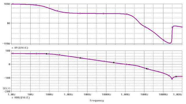 |
| Phase Margin simulation for a dual dominant pole and lead capacitor compensation scheme. |
|
|
Distortion Figures
 |
| Input and output spectrum for a 0.1Vmax 1KHz sinusoidal input signal. |
 |
| Input and output spectrum for a 0.9Vmax 1KHz sinusoidal input signal. |
 |
| Total Harmonic Distortion Simulation for the corresponding 0.1Vmax input signal at 1KHz. |
|
 |
| THD Simulation for the corresponding 0.9 Vmax input signal at 1KHz |
 |
| Speclab calibration input reference signal MEASURED spectrum |
|
|
 |
| MEASURED output spectrum and THD calculation |
|
Overall Comparison
 |
| Overall comparison between measured and simulated values in the design process |
|
Prototype Implementation
PCB Design
The pcb design must guarantee the correct connections of all the terminals of the active and passive components, and also account for their physical size to an optimal surface utilization. Design was carried out using the KiCAD software, and, though not optimal, a schematic based component distribution was prioritized in order to facilitate visualization and comprehension of the stages. A later PCB design can be optimized in terms of surface usage.
 |
| PCB Printout |
|
Grounding
Another thing to take into account are the grounding paths on the PCB. A star configuration was used, i.e. all grounding paths converge to a centralized grounding point. Nevertheless, paths for each important functionality were separated from each other in order to minimize unwanted interaction.
- Bias currents grounding
- Signal grounding
- Power stage grounding
This way the signal path is not affected by bias current or power stage noise, which are greater in orders of magnitude than those present on the small signal path itself.
Filtering Capacitors
Filtering capacitors were located at strategic points, of average values of 220 \( \mu F \)/50 V between voltage rails and bias paths to reduce possible rectification ripple provided by the power supply or other noises.
Diode-resistor circuits were placed as well to provide asymmetrical paths for the capacitors' charge-discharge cycles, inducing in turn asymmetrical rise and fall times. This further improves power supply peak immunity and avoids capacitor discharge through the load's grounding path.
Signal Path and Power Path
Routing track size is the determinant factor to differentiate signal and power paths. The tracks that manage more current are going to be consequently wider to offer a lesser resistivity and a lower power dissipation as a consequence. Track spacing is also taken into account due to possible eddy current capacitance that may be present in HF at high currents. Lastly, corners on the tracks were rounded to avoid charge accumulation and unwanted capacitive effects.
Heat sink calculation
The ensemble of the power transistors along with their temperature parameters and the heat sink compose a parallel of thermal circuits for which it is necessary to determinate its thermal resistance. The equation governing this effect is given by:
\begin{equation}
T_{max}-T_{min} = P_{max}(\theta_{jc} + \theta_{cd} + 2\theta_{d})
\end{equation}
where \( T_{max} \) is the maximum temperature of operation, supposedly 135ºC based on manufacture specs, and \( T_{max} \) of 40ºC the worst case room temperature. The juncture and package thermal resistance values are given by the manufacturer's datasheets of the MJE, these are \( \theta_{jc} = 16.7 ºC/W \) and 150ºC of juncture temperature. Thermal resistance of the mica/silicon grease interface used for thermal isolation is of \( \theta_{cd} = 0.5 ºC/W \) .
The transistors dissipation power is calculated as
\begin{equation}
P_{max} = \frac{V^2_{cc}}{\pi^2 R_{L}} = 14.6 W
\end{equation}
where maximal operating conditions were considered, given a load of 4 Ohm and +/- 24V supply rails.
Solving for \( \theta_{d} \) in the temperature resistance equation gives:
\begin{equation}
\theta_d = 2.2 ºC/W
\end{equation}
The ZD-7 heat sink, widely available on the market accounts for a thermal resistance of 2.1 ºC/W, which makes it suitable for this amplifier. Based on temperature measurements, a more exhaustive calculation can be carried out under normal operating conditions:
\begin{equation}
\theta_{ds} = \frac{54ºC - 29ºC}{14W} \approx 1.8 ºC/W
\end{equation}
which matches the manufacturer's specified value accordingly.
Component Technology
Carbon resistors were used with a tolerance of 5% to 10% depending the case. Even though a metal-film technology could have been used for the feedback network, subsequent measurements did not show any anomaly and the amplifier did not suffer from significant modifications in its behavior due to this omission.
Silicon diodes were chosen as to account for nominal bias current values and also to present a 0.6 V juncture voltage drop, which was the voltage value used for current source reference calculations.