Date: June 2010
Duration: 4 weeks
Author: Pablo Manuel Delgado
References:
[1] MacKenzie, S. The 8051 Microcontroller, Third Edici on, Prentice Hall.
[2] Datasheets for: AT89S52, 81C55, Winstar Display WH1602C-B, MAX232C,
CD74HC244E.
[3] MIDI Implementation Standard
[4] Messick, Paul. Maximum MIDI: Advanced music applications in C++, Manning Publications.
Video Demonstration
The main goal of this project was to design, develop and implement a MIDI based real time event sequencer with an 8051 microcontroller.
This device has the capability of communicating with other external equipment which support this protocol and establishing a synchronized execution of the diverse events on different machines by doing so.
The most well known application of this kind of devices is the cyclic sequencing and synchronization of different electronic musical instruments at a determined pace. Other applications include lightning and special effects for a great variety of performances.
The market price of a professionally available product of these characteristics is relatively high, so that special care was taken in proposing an economically viable and efficient alternative to these complex industrial solutions, a task specially suited for low cost microcontrollers in the 8051 family. Additional functionality was added:
- PC Device communication for sequence preloading.
- Protocol parameter configurability
Project description
Introduction
The sequencer's main function is that of executing diverse rigid patterns of events by utilizing an 8, 16 or 32 step grid. These patterns are chained and modified in real time in order to conceive complex compositions. The sequence is generally displayed with some indicator in the step matrix (see figure below). The number of rows can vary and it generally represents a fixed musical note or percussive element, the final row quantity will determine the amount of events that can be triggered at the same time. Due to the cyclic nature of this process, this device is usually utilized on the generation of rhythmic patterns and periodic musical phrases.
Communication with sequenced devices
One of the project's fundamental characteristics is that of inter-compatibility with different external agents to be operated. The device itself has not got any means of sound synthesis but acts as a mere event generator within the protocol standard. This communication is produced by using the micorcontroller's serial port with a software generated baud rate.
The MIDI (Musical Instruments Digital Interface) communication protocol is widely used within the industry and is a standard for event intercommunication between computers, synthesizers, sound cards, lighting devices and effect units. Signals created comprise volume changes, vibrato and signal panning, clock synchronization and tempo. Due to the great variety of implementations available, it is common practice for these devices to include a MIDI implementation table exactly specifying how these parameters are handled and communicated in every particular case.
Protocol's basic structure
The MIDI protocol consists on a start bit-stop bit serial interface communication for data transfer. It's baud rate is specified in 31250 symbols per second up to 1% of tolerance. Internally, MIDI comprises 16 channels (0 to 15) for media and control parameters multiplexing.
The basic structure used for the MIDI messages consists of 3 bytes. The first one being dedicated to system and channel messages (i.e. Channel 1, NOTE ON, Channel 3 NOTE OFF, hi of low nibble control type) and the second one containing the note number for the different octaves (coded onto 255 bytes). The third byte is dedicated to velocity and aftertouch for supporting devices.
For example: a "Note ON" message on Channel 1 (0 Nibble), 0x3C note (C3 on the tempered scale) with an intensity (aftertouch value) of 0x34 would be:
0900H 003CH 0034H
Features and Configurability
The following features are foreseen for the project:
Microcontroller choice and peripherals
 | |
| Figure 1: Step sequencer operation |
Communication with sequenced devices
One of the project's fundamental characteristics is that of inter-compatibility with different external agents to be operated. The device itself has not got any means of sound synthesis but acts as a mere event generator within the protocol standard. This communication is produced by using the micorcontroller's serial port with a software generated baud rate.
The MIDI (Musical Instruments Digital Interface) communication protocol is widely used within the industry and is a standard for event intercommunication between computers, synthesizers, sound cards, lighting devices and effect units. Signals created comprise volume changes, vibrato and signal panning, clock synchronization and tempo. Due to the great variety of implementations available, it is common practice for these devices to include a MIDI implementation table exactly specifying how these parameters are handled and communicated in every particular case.
 |
| Figure 2: Device interconnection example. |
Protocol's basic structure
The MIDI protocol consists on a start bit-stop bit serial interface communication for data transfer. It's baud rate is specified in 31250 symbols per second up to 1% of tolerance. Internally, MIDI comprises 16 channels (0 to 15) for media and control parameters multiplexing.
The basic structure used for the MIDI messages consists of 3 bytes. The first one being dedicated to system and channel messages (i.e. Channel 1, NOTE ON, Channel 3 NOTE OFF, hi of low nibble control type) and the second one containing the note number for the different octaves (coded onto 255 bytes). The third byte is dedicated to velocity and aftertouch for supporting devices.
For example: a "Note ON" message on Channel 1 (0 Nibble), 0x3C note (C3 on the tempered scale) with an intensity (aftertouch value) of 0x34 would be:
0900H 003CH 0034H
Features and Configurability
The following features are foreseen for the project:
- Text only LCD display and a multiple level menu for parameter configuration.
- LED based current state indicator.
- 4x8 keyboard with a logical state indicator for each button (on/off).
- Configurable tempo from 60 to 200 Beats Per Minute.
- Instrument type or MIDI note for each row.
- Volume control (after-touch).
- Serial port and USB port support for loading premade sequences from a personal computer.
Microcontroller choice and peripherals
Facing the diverse needs specified on the previous sections, a technical and market-related investigation was carried out in order to define which device would be the most suitable for this project and meet the most project requirements. The requirements, so to speak, were:
- At least three independent timers to generate robust sequencing, MIDI baud rate and serial/usb communication baud rate synchronization.
- Enough ROM memory for code storing, definitions and equivalency tables for tempo, menu items and configurable variables.
- Argentinean market availability and price.
- Is situ parallel programming capability, due to simplicity and cost.
- Great amount of available ports to handle the different ins and outs (keyboards, LED arrays, display, etc.).
It must be noted that there is not a single optimal choice for the microcontrolling device. There are at least two other suitable architectures for this kind of task. Nevertheless, the 8051 architecture has a vast amount of documentation and market availability. Albeit a steeper learning/programming curve, the fact that its low level (assembler) programming is specially well suited for real time application optimization was enough to ensure an overall robustness in the products performance. Many commercially available MIDI implementations lack this robustness and user response, and that is undoubtedly a determinant factor on the final product's quality.
Tempo and execution rate calculation
BPM and instruction execution rate
BPM and instruction execution rate
The execution pace of a musical sequence or piece is defined in Beats Per Minute (BPM). In order to set a proper correspondence between the timer's hardware interrupt ratio assigned for the step sequence pace and the BPM value, a BPM conversion formula was derived:
\alpha = \frac{60 \times 1MHz.}{BPM \times \beta}
\end{equation}
$$\alpha$$ is the amount of interruptions that occur before the processor's core moves on to the next step on the sequence and
$$\beta$$ is the reload rate of the timer per interruption.
For better precision, a data fitted version of the Beta parameter curve was used to show the hyperbolic function variations (Figure 3). The black curve represents the "continuous" values while the white ones represent the values implemented on the ROM equivalence lookup table.
 |
| Figure 3: Timer 0 interruption rate vs time. Real curve and lookup table values. |
- Protocol: MIDI Standard v1.0 and RS-232/USB
- Physical Interface: DIN5/180º connector, DB-9 Male Input
- Power Supply: 7-9 V (5v regulated internally), 250mA
- Display: 16 character alphanumeric x 2
- Keyboard: 4x8 push button matrix and LED binary indicator, Menu navigation, Play, Pause buttons
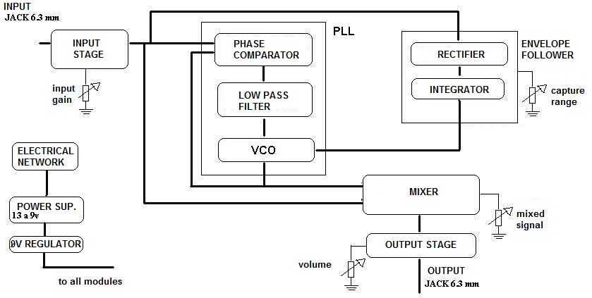
A comprehensive block diagram is shown on Figure 4. The core of the project is comprised by the microcontroller and the port expanders. The arrows show the data flow direction from device to peripherals.
 |
| Figure 4: Block Diagram |
Schematic Diagram
Figures 5, 6 and 7 show the electrical connection schematics for the microcontroller's printed circuit board, the matrix keyboard, the LED array and the menu keyboard respectively.
In order to ameliorate bus noise immunity on the LCD, pull up resistors were used on each bus connection to make the high and low logical states (voltage levels) more reliable.
At first, serial resistors were calculated for the LED array implementation. The leds on the matrix are not actually on all the time, but they blink on and off at a very fast rate on each microcontroller cycle depending on their logical state. As a consequence of this mode of operation, these previously calculated serial resistors limited the amount of intermittent current that was necessary to give the LEDs a proper brightness, so they were omitted on the final stage of the design.
The MIDI interface was established by means of a current loop specified in the MIDI standard. An impedance matching buffer on the 89S52 serial output was used.
PCB
Figures 8, 9 and 10 show a possible design of the printed circuit board. Experimental prototyping boards were used for the first design stages, with the exception of the matrix keyboard and LED, which designs were directly applied onto PCBs after a software schematic/layout matching test.
At first, serial resistors were calculated for the LED array implementation. The leds on the matrix are not actually on all the time, but they blink on and off at a very fast rate on each microcontroller cycle depending on their logical state. As a consequence of this mode of operation, these previously calculated serial resistors limited the amount of intermittent current that was necessary to give the LEDs a proper brightness, so they were omitted on the final stage of the design.
The MIDI interface was established by means of a current loop specified in the MIDI standard. An impedance matching buffer on the 89S52 serial output was used.
 |
| Figure 5: Microcontroller connection diagram. |
 |
| Figure 6: Matrix keyboard and led connection diagram. |
 |
| Figure 7: Menu navigation keyboard connection diagram. |
PCB
Figures 8, 9 and 10 show a possible design of the printed circuit board. Experimental prototyping boards were used for the first design stages, with the exception of the matrix keyboard and LED, which designs were directly applied onto PCBs after a software schematic/layout matching test.
 |
| Figure 8: Main board PCB layout. |
 |
| Figure 9: Matrix keyboard and LED array PCB layout. |
 |
| Figure 10: Menu navigation keyboard PCB layout. |
Memory Mapping
The external RAM memory mapping is comprised of the memory addresses offered by the 81C55 port expander IC's. Although the internal expander memory was not used in the end, a decision was made to include on the overall project memory design and addressing in case of a future firmware update/product expansion without any hardware modification.
Code Walkthrough
Initializations
The code consists of a series of initializations that can be divided onto three categories:
The external RAM memory mapping is comprised of the memory addresses offered by the 81C55 port expander IC's. Although the internal expander memory was not used in the end, a decision was made to include on the overall project memory design and addressing in case of a future firmware update/product expansion without any hardware modification.
 |
| Table 1: Internal Memory Mapping of the 81C55 port expanders. |
 | |
|
Code Walkthrough
Initializations
The code consists of a series of initializations that can be divided onto three categories:
- Port expanders
- LCD display
- Memory allocation for program variables
The 81C55 port expanders need a proper initialization in order to be properly used. From the microcontroller's point of view, these are no other than external memory addresses. In turn, these expanders have 255 bytes of RAM memory, a timer, two input/output ports (8 bits) and a third 6 bit communication port. The initialization routine writes a "Command Register" byte that specifies the expander's mode of operation, including port functionality and timer. This "command register" byte can be modified at any time of the main program execution.
LCD Display:
A standard initialization routine proposed by the manufacturer is used. This routine is called twice in the code, in order to ensure that the proper values were set for the LCD display, this procedure was determined empirically. The routine's complexity was given by the proper access/write time management due to the fact that this device's frequency of operation orders of magnitude lower than the microcontroller's (270 KHz vs. 12 MHz.)
Variable Initialization:
This routine is just for setting preloaded variable values for the rest of the code. Some subroutines need some variables written on a specific physical address, as well as pre cleansing of memory allocation spaces to avoid garbage information to be permeated on some of the devices' initialization.
Main Routine
As both the sequence and the 89S52 input port comprises of 8 steps and pins respectively, it logically follows that each step (matrix column) can be read directly from an input port pin. The matrix keyboard consists of 5 rows and 8 columns as well. The four first button rows correspond to the step sequencer and the last row is assigned to the menu navigation keyboard.
First, the row to be read is addressed by putting a logical zero on the correspondent input pin. Next, the port corresponding to each column is read, a logical zero is assigned each time a button remains pressed. This byte is then complemented and stored into the RAM in an auxiliary array. This method is used because the keyboard is read twice in total, and a logical comparison between the first reading and the second one is performed. In case that the second reading matches the first one, it is considered that the button is on the correct state. This is made so to avoid incorrect state transitions due to the bouncing voltage effect on the push buttons.
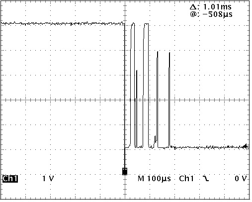 | ||||
Example of a contact's bouncing voltage measurement.
|
The comparison is performed on an AND logical gate between the stored readings and the new ones. The state transition update is made by an XOR logical gate with the keyboard's values previously stored. This is made so because the push button logical state is held by software.
A difficult task to accomplish was that of having to read the push button twice with a minimum idle time (approx 10 ms to wait for the bouncing time transient) without having to stop the main routine, due to the real time constraints of the performance. This problem was solved by the use of flag bits and a decrementing auxiliary variable that changed its value each time the processor's core performs a full running cycle.
A difficult task to accomplish was that of having to read the push button twice with a minimum idle time (approx 10 ms to wait for the bouncing time transient) without having to stop the main routine, due to the real time constraints of the performance. This problem was solved by the use of flag bits and a decrementing auxiliary variable that changed its value each time the processor's core performs a full running cycle.
The algorithm for the push button interaction is described as follows:
- Read the button's current state. Set flag for the first reading. The first reading won't be repeated until this flag is set low again (first reading semaphore).
- Wait for the main program loop to decrement the auxiliary variable until it reaches the zero value. (this is equivalent to waiting a prudential time for the second reading)
- Read the keyboard matrix a second time. Set flag for the second reading. The second reading won't be repeated until this flag is set low again (first reading semaphore).
Menu
The menu consists, broadly speaking, of two parts:
- Parameter selection to be modified.
- Modification of the parameter itself.
Here is another video capture showing different parameter configurations via menu navigation. It is also shown how the real time communication with the PC works on loading pre-arranged patters from a file.


